Settings
 Fast Delivery
 Payment Types


 Marketplace Product

Selecting Components for Fast-Transient, Wide-Range Current Sensing in AI Datacenters
Contributed By DigiKey's North American Editors
2026-09-29
Measuring the current flow between a power source and a load, whether a motor, circuit board, or rack, is an increasingly important system-level requirement that enables power optimization at the system and subsystem levels. While components for current-sensing circuits are well established across various configurations, the growth of artificial intelligence (AI) datacenters has made this function more challenging. Current levels are higher and span a wide dynamic range, with rapid transitions between minimum and maximum levels that must be accurately measured.
Meeting these heightened requirements requires careful selection of analog and mixed-signal components within the established circuit topologies.
This article discusses the need for current sensing and the challenges posed by AI datacenters. It then provides an overview of a circuit design and examines the use of off-the-shelf analog/mixed-signal components from Analog Devices that can be applied to address these challenges.
Establish system-level goals
While each AI datacenter is different, there are general guidelines that can be used to establish the system-level current-sensing requirements, including:
- Maximum system current: one kiloampere (kA), distributed across multiple circuit boards, each with multiple graphics processing units (GPUs)
- Readout dynamic range: greater than 90 decibels (dB)
- ADC resolution: at least 16 bits, with 18 to 20 bits preferred
- Linearity: ½ least significant bit (LSB) at the 16-bit level; integral nonlinearity below ±8 parts per million (ppm)
- Settling time: less than 50 nanoseconds (ns) at the 16-bit level
Sizing the sense resistor
One of the first design tasks is sizing the current-sense resistor to match each board’s specifications. For example, consider a circuit board that draws a maximum of 3 A with eight AMD Radeon GPUs, or approximately 375 mA to 400 mA per GPU. This current is split roughly evenly between the 1.8 V and 0.9 V rails, so the current to be sensed on each rail is about 200 mA full-scale (FS).
Responsible engineering practice in this scenario indicates that a voltage drop of about 50 mV is the maximum acceptable drop, or “burden” voltage across the current-sensing resistor. Using Ohm’s Law, this corresponds to a maximum resistance of 250 mΩ. A good choice that provides extra headroom and reduces loss is 100 mΩ.
Once the sense resistor’s FS voltage is known, the rest of the design and component selection can proceed. With a 200 mA FS current through the 100 mΩ shunt resistor, the FS voltage across that resistor that needs to be captured and amplified is 20 mV.
A simplified schematic of the circuit (Figure 1) shows four primary functions:
- An instrumentation amplifier (in-amp) to sense, condition, and scale the small voltage developed across the sense resistor (Rsense)
- A differential amplifier that accepts the in-amp output and conditions it for the analog-to-digital converter (ADC)
- An ADC that digitizes the signal with high accuracy, high resolution, and low noise
- A precision voltage reference for the ADC
 Figure 1: A simplified schematic diagram shows the critical functions in the signal chain from the current-sense resistor to the final digitized output. (Image source: Analog Devices)
Details of the current-sense circuit
The in-amp: Given the relatively low FS voltage, the required resolution, and the likely impact of internal component noise on readings, a suitable in-amp choice is the AD8421ARZ. This amplifier features a maximum input voltage noise of 3.2 nV/√Hz and 200 fA/√Hz current noise at 1 kilohertz (kHz) (Figure 2, left). It has a maximum bandwidth of 10 megahertz (MHz), a common-mode rejection ratio (CMRR) of 94 dB at a gain of 1 (G = 1), and flat gain versus frequency up to the roll-off frequency (Figure 2, right).
 Figure 2: The AD8421ARZ instrumentation amplifier features low current noise (left) and flat gain versus frequency up to the roll-off frequency (right). (Image source: Analog Devices)
With its gain set to 10 V/V via Rgain of 1.1 kΩ, the output is 200 mV peak-to-peak (VP-P), and the full 3 dB bandwidth of 10 MHz is maintained. The amplifier’s input-referred noise at this bandwidth exceeds that of the subsequent ADC.
The differential amplifier: The next step is to condition the amplified sense-resistor signal so it can interface with the ADC. For this role, the ADA4945-1ACPZ-R7 fully differential ADC amplifier/driver is a good fit. It features a ±0.1 µV/°C offset drift, which is critical for stability and consistent performance. Differential signaling minimizes noise effects and maintains performance in the presence of common-mode voltages.
At a gain of one, the ADA4945-1ACPZ-R7 has a typical small-signal bandwidth of 80 MHz in low-power mode and 145 MHz in full-power mode, as selected by the user. It also features low voltage and current noise and a fast settling time (Figure 3), ensuring accurate acquisition of rapidly changing signals.
 Figure 3: The ADA4945-1ACPZ-R7’s fast settling time enables accurate acquisition of rapidly changing signals. (Image source: Analog Devices)
Setting the ADA4945-1ACPZ-R7’s gain to 7.02 V/V matches its output span to the next stage’s input range, optimizing performance and minimizing noise contribution.
The ADC: Digitization of the voltage signal that represents the sensed current is the broad system-level objective, and implementing that is the function of the ADC. The AD4084BBCZ-RL7 (Figure 4) is a good choice here. This highly integrated successive approximation register (SAR) ADC features low noise (8.8 nV/√Hz), low power (80 milliwatts (mW) at 40 megasamples per second (Msamples/s)), high dynamic range (94.6 dB), and excellent typical linearity of ±4 parts per million (ppm). It also includes a 16 kilosample first-in, first-out (FIFO) result data buffer with event detection, which greatly reduces the immediate load on the digital host.
 Figure 4: The AD4084BBCZ-RL7 SAR ADC's integrated functions reduce the need for external support circuitry. (Image source: Analog Devices)
The AD4084BBCZ-RL7’s Easy Drive features reduce signal chain complexity and power consumption while enabling greater channel density and flexibility in selecting companion components. Its reduced bandwidth requirement also enables the use of lower-power drivers.
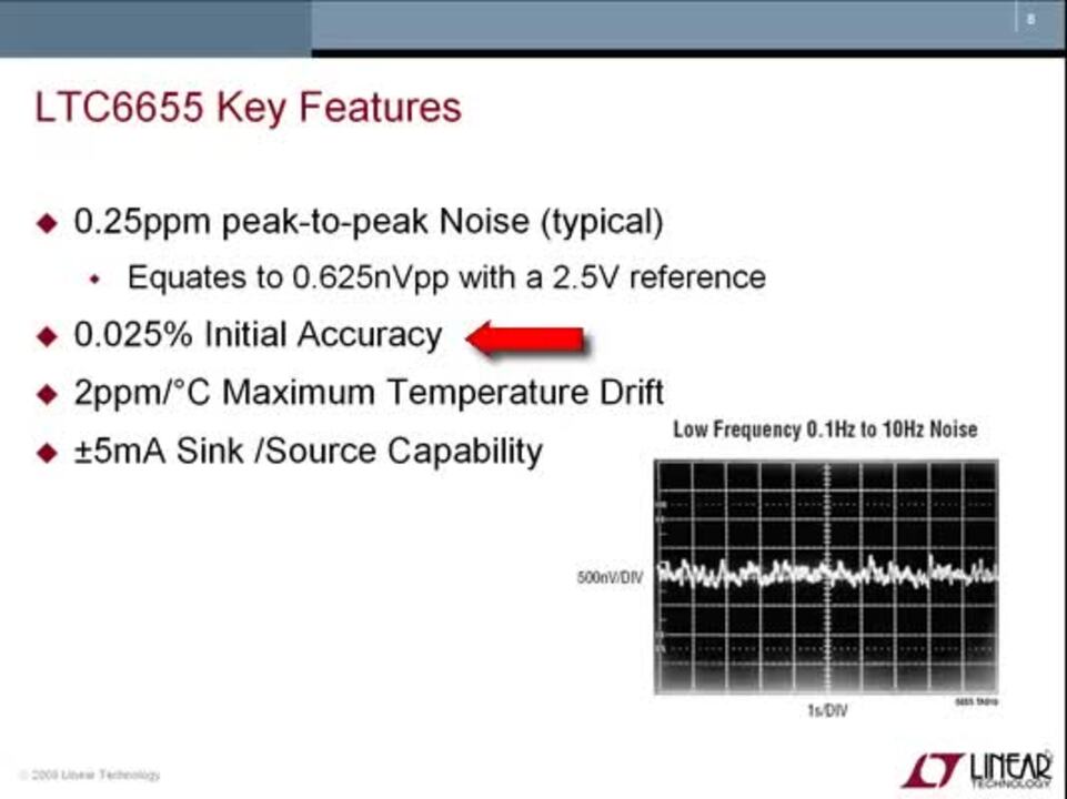
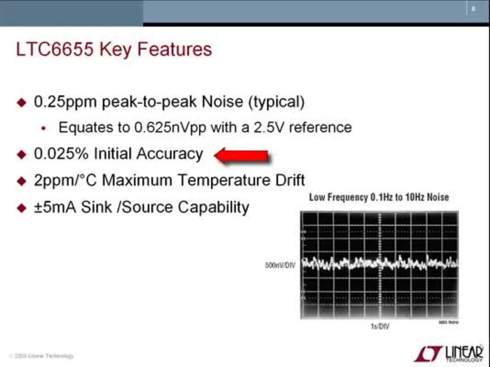
The voltage reference: Some ADCs include an internal reference, which can be quite good. However, a standalone voltage reference, such as a 3 V version of the LTC6655, is a better choice for accurate, stable, and consistent signal-chain performance.
The LTC6655 features 1/f noise below 625 nV peak-to-peak (nVP-P) (Figure 5, left), drift below 2 ppm/°C (Figure 5, right), and absolute accuracy of ±0.025%. As a result, it provides a precise, stable reference for the entire current-measurement signal chain.
 Figure 5: The LTC6655 voltage reference combines extremely low noise (left) with extremely low temperature drift (right) for precision performance. (Image source: Analog Devices)
Optimizing the design
Every design balances factors such as performance, board space, power consumption, and cost, and this design is no exception. Another factor is dynamic range. The circuit as shown offers dynamic range above 60 dB and an input-referred noise of about 200 microamperes (µA), which is good but still below the original 90 dB target.
Among the steps that can be taken to increase this figure are to decrease the front-end gain in the AD8421ARZ in-amp and increase the integrated digital filtering (decimation) available in the ADC by a factor of four or even eight, which will increase the dynamic range by 6 dB and 12 dB, respectively, but at the cost of conversion rate.
This change in gain does not require hardware replacement. Instead, gain switching can be implemented at the AD8421ARZ using an analog switch, such as the ADG5404FBRUZ-RL7 4-channel multiplexer, which features a typical on-resistance of 10 ohms (Ω).
However, analog switches have inherent parasitics, such as the cited on-resistance and other nonlinearities, that make them less suitable for high-precision measurements. Their performance in this regard would need to be evaluated through careful signal-chain modeling and simulation. For this reason, using a low-noise, wide-dynamic-range ADC, such as the AD4084BBCZ-RL7 without gain ranging, may be the better choice because it simplifies the signal chain and removes sources of error.
For applications where space is at a premium or the bill of materials (BOM) must be minimized, the more highly integrated AD4884BBCZ-RL (Figure 6) is an alternative to the AD4084BBCZ-RL7 ADC. This dual-channel, low-noise, low-power, high-speed, 16-bit SAR ADC includes fully differential amplifier (FDA) drivers and gain-setting resistors.
 Figure 6: The AD4884BBCZ-RL ADC is an alternative to the AD4084BBCZ-RL7, helping reduce board space and BOM cost. (Image source: Analog Devices)
Its two channels can be sampled either simultaneously or independently, offering flexibility for a wide range of applications. Optimized for input signals up to 1 MHz, the AD4884BBCZ-RL features exceptional linearity and extremely low power consumption, making it a viable alternative for many precision data-acquisition systems.
Conclusion
Accurate current sensing in AI datacenters requires a signal chain capable of handling high current, a wide dynamic range, and rapid load transitions. A successful design requires careful component selection and signal-chain optimization to balance accuracy, noise, response time, board space, power consumption, and circuit complexity. Analog Devices offers instrumentation amplifiers, differential ADC drivers, SAR ADCs, voltage references, and integrated alternatives to implement the required functions.

Disclaimer: The opinions, beliefs, and viewpoints expressed by the various authors and/or forum participants on this website do not necessarily reflect the opinions, beliefs, and viewpoints of DigiKey or official policies of DigiKey.